“The LTC3649 is a single-chip step-down regulator that can operate from an input voltage range of 3.1 V to 60 V, and can efficiently generate a single resistor programmable output voltage at an output current of up to 4 A. These characteristics alone make it an attractive industrial or automotive power supply with an output voltage from VIN C 0.5 V to ground. A unique feature of the LTC3649 is the ability to power critical systems when the power is off, without any additional components.
“
Victor Khasiev Senior Application Engineer, Analog Devices
The LTC3649 is a single-chip step-down regulator that can operate from an input voltage range of 3.1 V to 60 V, and can efficiently generate a single resistor programmable output voltage at an output current of up to 4 A. These characteristics alone make it an attractive industrial or automotive power supply with an output voltage from VIN C 0.5 V to ground. A unique feature of the LTC3649 is the ability to power critical systems when the power is off, without any additional components.
When the power rail fails, the holding Circuit powers the critical system, enabling it to perform important management tasks such as data retention within a short period of time before all available energy is lost. Typical holding solutions use dedicated controllers and large storage capacitors, 1, 2 such as LTC3310 and LTC3643. Therefore, if the critical circuit requires a lot of power and hold time, the cost and complexity will increase. But if the required holding energy is relatively low, the LTC3649 can easily perform this task without the need for additional Circuits.
The dual-output converter described here is used as a traditional step-down power supply under normal operating conditions, but during a power interruption, the converter itself becomes an energy source and maintains a set output voltage for key circuits. To perform this task, when the input voltage is disconnected, U1 becomes a boost converter, which causes U1 to discharge its output capacitor to provide holding energy.
Dual output converter and hold circuit
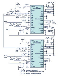
Figure 1 shows the retention design using LTC3649. Under normal conditions, the unregulated voltage rail VIN (VINS through the blocking diode) powers the U1-based converter (Converter A). The converter works in step-down mode and generates a stable 5 V voltage on VOUT1. VINS is connected to the second converter (converter B) based on U2, which supplies 3.3 V to the critical load on VOUT2. When VIN fails, converter A enters the boost mode and maintains its set output voltage (VINS) by discharging its output filter capacitors C01 and C02. The resistors RIT and RIB set this voltage level. The PGOOD (PG) signal generated by U1 can be used to transmit power failures to the system, thereby disconnecting non-critical circuits to maintain energy. The MODE/SYNC pin will be left floating to allow the LTC3649 to enter the boost mode.

Figure 1.5 V output converter (U1) supplies and maintains power to the protected load on the 3.3 V output (U2).
Please note that the pin MODE/SYNC of U1 will be left floating to allow the LTC3649 to enter the boost mode.
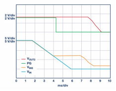
Figure 2 shows the operation of the LTC3649 in boost mode. For the first 7 ms of capture, all voltages are stable. At 7 ms, the power is turned off; both VIN and INS begin to drop. When VINS reaches 8 V, it stabilizes and the PG signal changes state, indicating that VOUT1 begins to collapse. As long as C01 and C02 are charged, VINS remains at 8 V. VOUT2 remains constant throughout the process, providing a stable power supply for critical loads for a long time after the power supply is interrupted. ADI has created LTspice®Model.

Figure 2. When the input voltage VIN drops, converter U1 boosts VOUT1 to maintain VINS at 8 V.
After VIN is stepped down, VINS supplies power to keep VOUT2 stable for more than 20 ms.
in conclusion
LTC3649 is a monolithic step-down regulator with integrated power MOSFET. It has high efficiency and low quiescent current, which is very important in many battery-powered systems. It also has high versatility, programmable frequency, a wide VIN range up to 60 V, and an output voltage range as low as ground. It simplifies the design of automotive and industrial products, especially when considering its potential as a holding circuit.
About the Author
Victor Khasiev is a senior application engineer at ADI and has extensive experience in the field of power electronics for AC/DC and DC/DC conversion. He holds two patents and authored many articles. These articles deal with the use of ADI semiconductor devices in automotive and industrial applications, including boost, buck, SEPIC, positive-to-negative, negative-to-negative, flyback, forward converters, and bidirectional backup power supplies. His patents are related to high-efficiency power factor correction solutions and advanced gate drivers. Victor is happy to provide support to ADI customers, answer questions about ADI products, power supply schematic design and verification, printed circuit board layout, troubleshooting, and participate in testing the final system. Contact information:[email protected]