Power semiconductor devices have been developing since the 1950s and have evolved into a multi-generation product system represented by diodes, thyristors (SCRs), MOSFETs, IGBTs, and other components. The emergence of new technologies and products has expanded the application scope of existing products and technologies to meet the demands of various end products. For instance, MOSFETs have evolved into using new materials like GaN and SiC to cover applications requiring higher power density, higher voltage, and faster switching speeds. MOSFETs exhibit the characteristic of coexistence across multiple generations. This article aims to calculate the actual losses of MOSFETs in practical applications using parameters from datasheets, providing design engineers with reference values for selecting appropriate components.
The power losses of a MOSFET operating in switching mode can be categorized into three types:
Hence, the losses in a MOSFET operating in switching mode are as follows:

Conduction Loss (Pc)
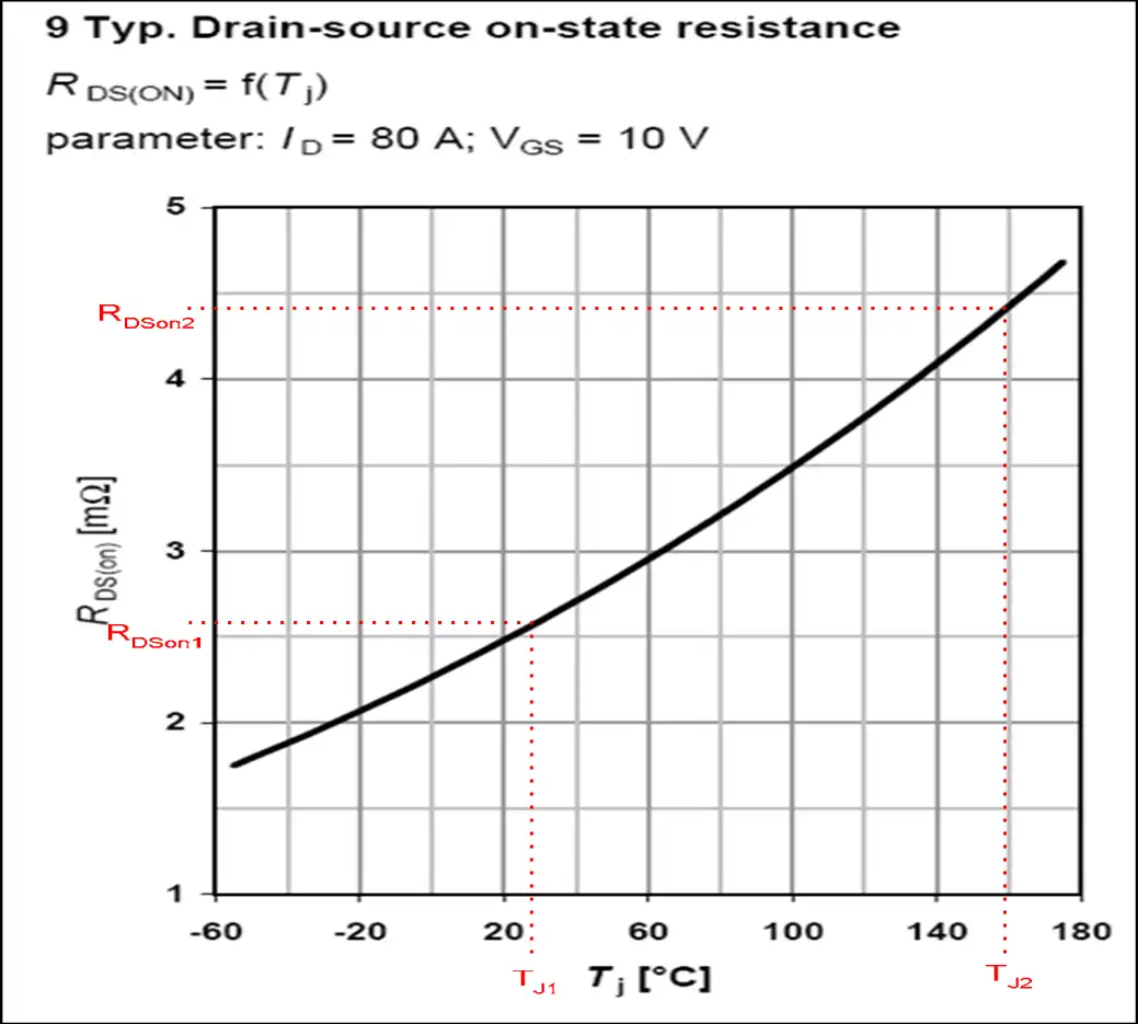
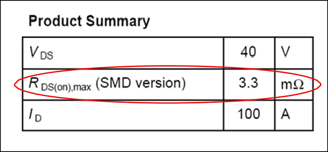
The losses in a power MOSFET can be approximated using the on-resistance (RDSon) of the MOSFET in its conduction state:

Where UDS is the drain-source voltage and ID is the drain current.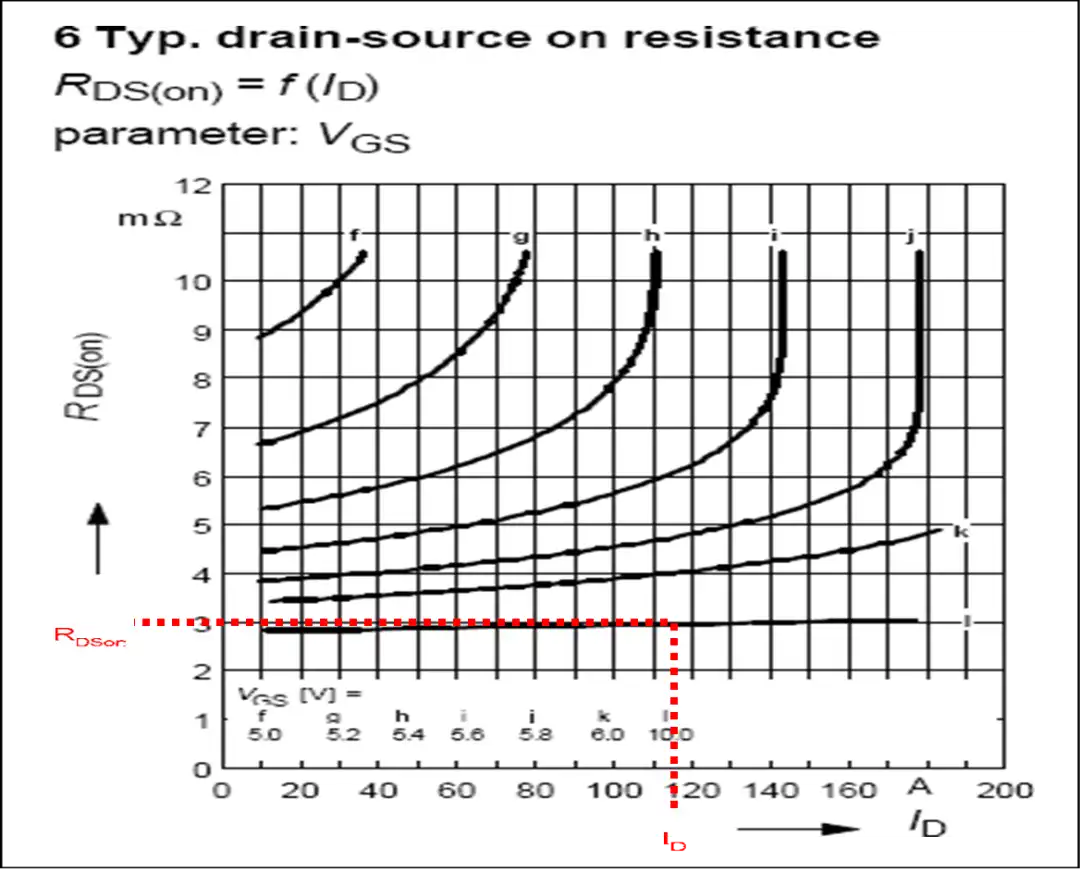
Typical RDSon values can be obtained from the datasheet as shown in Figure 1, where ID is the MOSFET’s conduction state current.
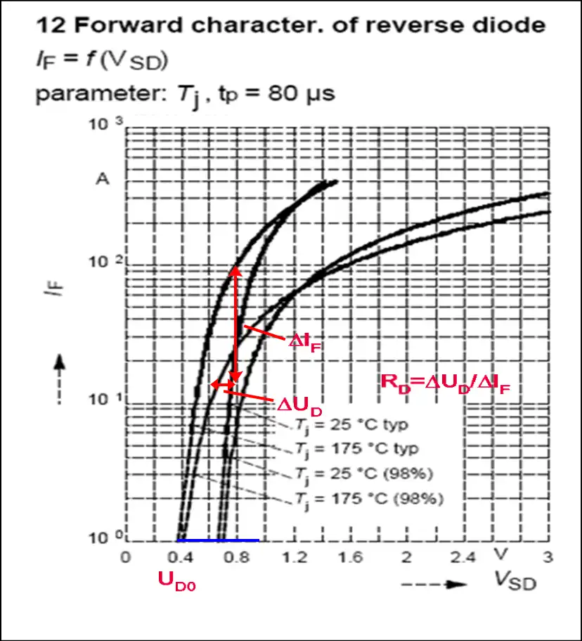
The conduction loss of the anti-parallel diode can be estimated using a diode approximation, considering a voltage source (uD0) representing the diode’s zero-current voltage and a series connection with the diode’s on-state resistance (RD). If the current through the diode is IF:
![]()
These parameters can be obtained from the MOSFET datasheet charts, and for conservative calculations, the uD0 value obtained from the chart must be scaled by (UDmax/UDtyp). These precise values can be read from the datasheet, or typical safety margin values (10%-20%) can be used for practical calculations.
The average diode current IFav and the root mean square diode current IFrms give the average diode conduction loss within the switching period (Tsw = 1/fsw):

Switching Loss (Psw)
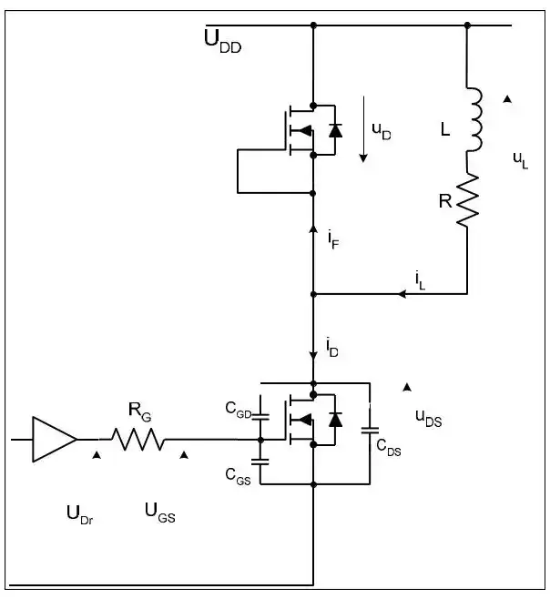
The circuit used to check MOSFET switching loss is shown in Figure 5. It is a single-quadrant chopper supplying an inductive load. The MOSFET is driven by a driver circuit, providing a voltage UDr at its output. The internal diode of the MOSFET acts as the freewheeling diode. In most applications, the entire topology consists of one or more MOSFET-based half-bridges, such as in three-phase AC motor drives, DC motor drives, synchronous DC/DC converters, etc. If an external freewheeling diode is used, it can be extracted from the diode datasheet, and the calculation still holds.
For the calculation of power loss, a linear approximation of the MOSFET switching process is sufficient, which represents the worst-case scenario for calculations. The ideal MOSFET switching process is shown in Figure 6. Part (A) at the top represents the gate-source voltage (uGS) and gate current (iG); the next one (B) shows the drain-source voltage (uDS) and drain current (iD), neglecting the reverse recovery of the freewheeling diode. Part (C) gives a qualitative overview of power loss, and part (D) shows the influence of reverse recovery on switching loss.
The driver circuit changes its state from 0V to UDr, raising the gate voltage to the threshold voltage (UGS(th)), with a time constant defined by the gate resistor and the equivalent MOSFET input capacitance (Ciss = CGD + CGS). The output won’t change until the gate voltage reaches UGS(th).
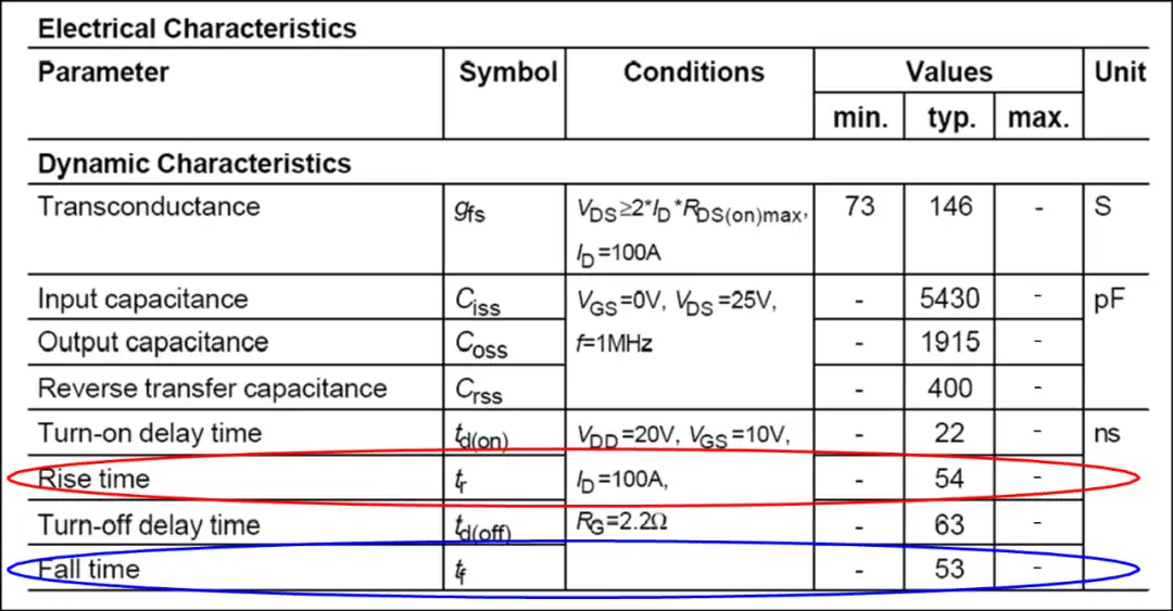
After reaching UGS(th), the drain current rises, taking over the load current. The rise time (tri) between zero and IDon (defined by the application) can be read from the MOSFET datasheet as shown in Figure 7. During the current rise, the freewheeling diode is still conducting, and the drain-source voltage is UDD.
To turn off the diode, all minority carriers in it must be removed (see Figure 6). This reverse recovery current must be absorbed by the MOSFET, resulting in additional power loss. The worst-case values for reverse recovery charge (Qrr) and time (trr) used in power loss calculations can be obtained from the MOSFET datasheet (see Figure 8).
After the diode turns off, the drain-source voltage drops from uDS = UDD to its on-state value uDS = RDSon * Ion. The Miller effect occurs, clamping the gate-source voltage at uGS = U(platform) (see Figure 9).
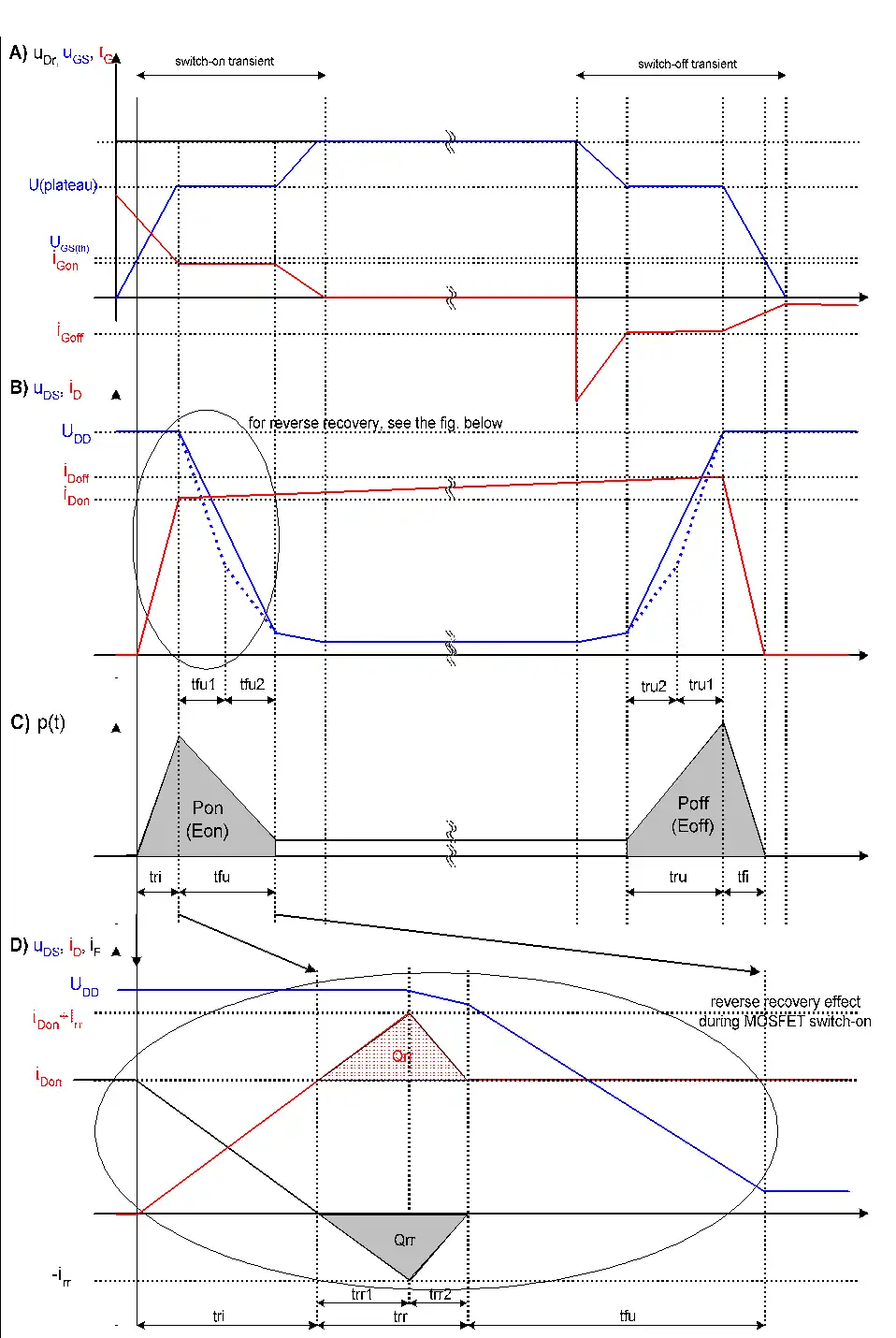
The slope of the drain-source voltage during this phase is determined by the gate current flowing through the gate-drain capacitance (CGD = Crss). To compute the voltage drop time (tfu) with reasonable accuracy, the nonlinearity of the gate-drain capacitance must be considered. Figure 10 depicts the typical dependency of gate-drain capacitance on drain-source voltage.

This nonlinearity is not easy to incorporate into calculations, which is why the two-point approximation is used. Assuming the drain-source voltage is within the range of uDS [UDD/2, UDD], the value of the gate-drain capacitance is CGD1 = CGD(UDD).
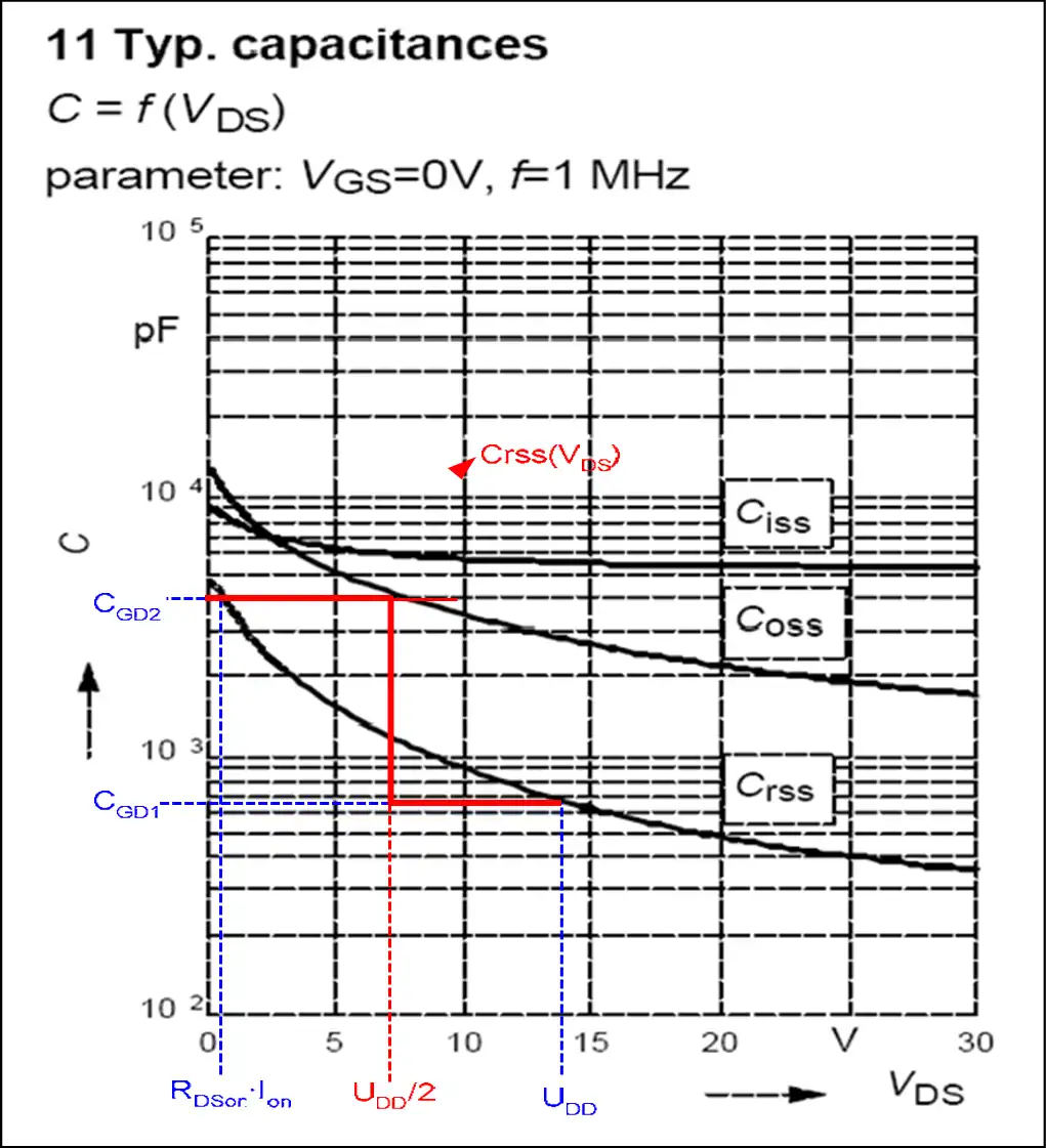

On the other hand, if the drain-source voltage is within the range of uDS [0V, UDD/2], the gate-drain capacitance value is CGD2 = CGD(RDSon * Ion). The determination of these capacitance values is illustrated in Figure 10. The dashed line in Figure 6B represents the drain-source voltage during the voltage drop, considering the two-point approximation.

This approximation is used solely for determining the voltage drop time (and the rise time during turn-off) and assumes a linear form of the drain-source voltage (represented by the solid line in Figure 6B), thus presenting the worst-case scenario for the switching loss analysis.
The gate current during tfu can be calculated as:

The voltage drop time can be calculated as the midpoint of the falling times defined by the gate current and the capacitances CGD1 and CGD2.

Switching Energy and Loss
Based on the earlier considerations, the worst-case conduction energy loss (EonM) of the
