[Introduction]DC-DC boost circuits are very common in Electronic circuits. Whether it is to match the working voltage of different devices or to improve enough output power, a boost circuit must be used. Especially for portable electronic products, the power source is battery-powered, such as single-cell lithium battery, three-cell lithium battery or lead-acid battery 12V. Through the DC-DC boost circuit, it can supply power to other circuits after boosting.
The boost chip is a switching circuit, and the most critical indicators are the input MOS switch tube current, output voltage value, boost output current and efficiency. The built-in MOS tube integrated chip DC-DC booster integrated circuit below 70W is very mature. For example, the DC-DC booster IC in the SOT-23 package on the market is boosted from 3.7V to 12V, and the maximum input current is generally within 3A; the DC-DC booster in the SOP8 package is generally less than 3A. – The maximum current of the built-in switch tube of the DC boost IC is 10A, but the maximum output voltage is 12-13V.
Shenzhen Yongfukang Technology Co., Ltd. promotes a 17.8V output, high-current asynchronous DC-DC boost IC with an integrated 14A switch tube for DC-DC boost application requirements with a boost value below 18V: HT7181. HT7181 adopts unique circuit research and development technology and advanced semiconductor process. Based on eSOP8 package, the working efficiency is as high as 92%, and no external heat sink is required; the pin function is compatible with the previously launched HT7180, and the performance is upgraded while realizing seamless switching of circuit design. .
1. HT7181 overview
The HT7181 is a high-power non-synchronous boost converter with integrated 20mΩ power switch, providing an efficient and small-footprint solution for portable systems. The HT7181 has a wide input voltage range of 2.7V to 16V and can support applications using single or two-cell Li-Ion batteries, or 12V lead-acid batteries. The device has 14A switching current capability and can provide output voltages up to 17.8V. The HT7181 also supports programmable soft-start, and adjustable switch peak current limit. The HT7181 also supports two different tr/tf to accommodate different EMI and efficiency requirements. In addition, the device also provides 18V output overvoltage protection, and thermal shutdown protection.
2. Features of HT7181
● Input voltage range: 2.7V-16V
● Output voltage range: up to 17.8V
● Fixed switching frequency: 360kHz
High conversion efficiency:
● 83% (VIN = 3.7V, VOUT=9V, IOUT =2.7A)
● 83% (VIN = 3.7V, VOUT=12V, IOUT =2.5A)
● 82% (VIN = 3.7V, VOUT=16V, IOUT =1.5A)
● 91% (VIN = 3.7V, VOUT=12V, IOUT =1A)
● 92% (VIN = 7.4V, VOUT=13V, IOUT =5A)
● 94% (VIN = 7.4V, VOUT=13V, IOUT =3A)
● 90% (VIN = 7.4V, VOUT=16V, IOUT =4A)
● 93% (VIN = 7.4V, VOUT=16V, IOUT =1.5A)
● Low shutdown power consumption, shutdown current 1uA
● Support two tr/tf modes to deal with EMI challenges
● Programmable soft start
● Output overvoltage (18V), thermal shutdown and other protections
● eSOP8L-PP lead-free package
3. Application of HT7181
● Drawbar speakers, portable speakers, wireless speakers
● Charging device, power bank, USB TYPE-C power transmission
● Tablet PC, Notebook PC・POS Terminal
4. Typical application parameters
The typical parameters of HT7181 used in single-cell lithium battery boost, double-cell lithium battery boost, and three-cell lithium battery boost are as follows:
● The single-cell lithium battery 3.7V is boosted to 9V/3.33A/30W.
● Single-cell lithium battery 3.7V application boost to 12V/2.5A/30W.
● Single-cell lithium battery 3.7V application boost to 16V/1.88A/30W.
● Double-cell lithium battery 7.4V is boosted to 13V/5.38A/70W.
● Double-cell lithium battery 7.4V is boosted to 16V/4.38A/70W.
● Three-cell lithium battery 12V application boost to 16V/7.5A/120W.
Single-cell/dual-cell/three-cell lithium battery application boost output voltage/current/power and set resistance value corresponding to FB pin:

5. HT7181 Application Information
(1). HT7181 pin map
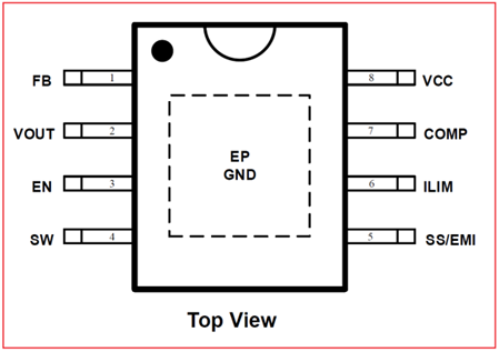
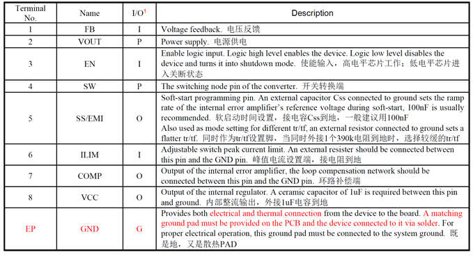
(2).HT7181 pin description
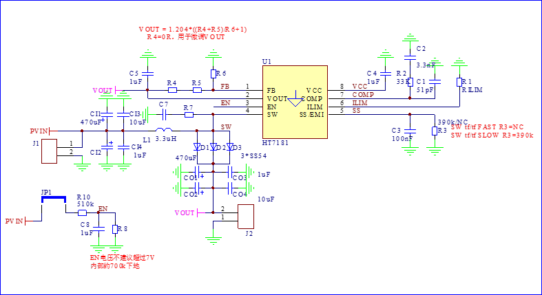
(3). Schematic diagram of HT7181 DEMO board
(4). HT7181DEMO board PCB top layer design
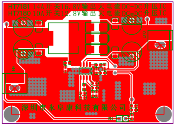
(5). HT7181DEMO board PCB bottom layer design
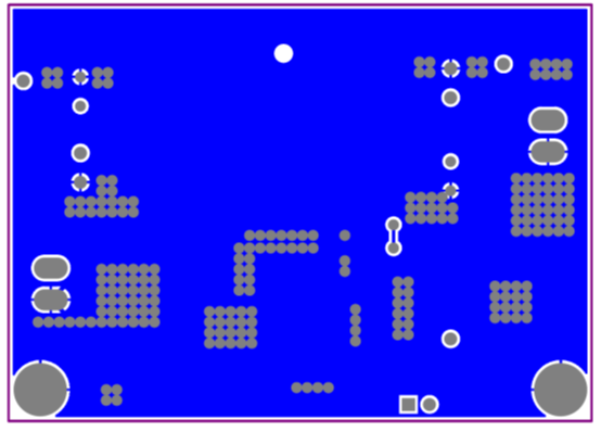
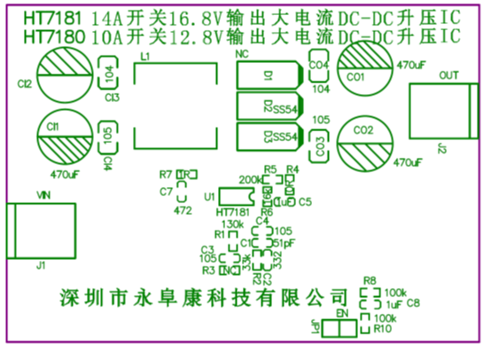
(6). HT7181DEMO board patch picture
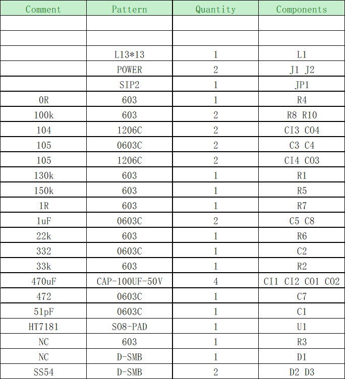
(7). HT7181DEMO board bill of materials
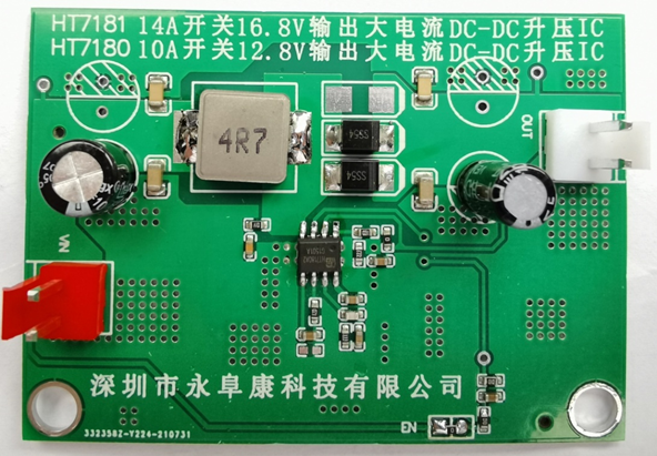
(8). Physical map of HT7181DEMO board
The Links: G150XNE-L03 VI-2T0-EW