In bus communication, the MCU in the bus device needs to connect a bus transceiver to the bus network. What happens if the power supply voltage of the MCU does not match the transceiver voltage? This article will take CAN bus as an example to analyze the importance of level matching from the perspective of interface level.
CMOS level
Most digital integrated circuits now use CMOS technology, and the level of its interface roughly conforms to the following definitions:
VIL0.7Vcc;
VOL0.9Vcc.
Taking common 5V and 3.3V systems as an example, the corresponding interface parameters are shown in Table 1.

Table 1 Level requirements under different power supplies
Note: The data in the table is only a reference value for calculation, and the actual parameters of the device should refer to the corresponding data sheet.
level mismatch
To ensure reliable signal transmission between the two devices, it must be ensured that:
The VOH(MIN) of the driver output must be higher than the VIH(MIN) of the receiver input.
The VOL(MAX) of the driver output must be lower than the VIL(MAX) of the receiver input.
The output voltage of the driver output must not exceed the I/O voltage tolerance of the receiver input.
When two CMOS devices are connected together, if the supply voltage is the same, there is no problem in signal transmission. If the supply voltages of the two devices are inconsistent, there will be a level mismatch problem.
Taking the connection of a 3.3V device and a 5V device as an example, the following two problems will occur:
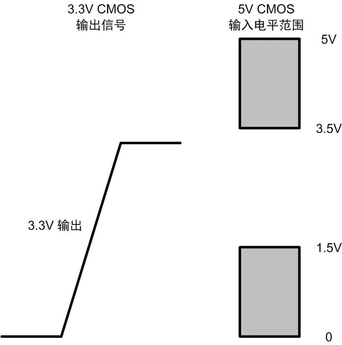
The input pin of 5V device may not recognize the high level output by 3.3V device. As shown in Figure 1, the maximum value of VOH output of 3.3V device is 3.3V, and the minimum value of VIH of 5V device cannot reach 3.5V, and the high voltage output of 3.3V device cannot be guaranteed. Flat is correctly identified. Due to the margins in the device design, it may still work when tested, but there is a risk that problems can arise if the device voltage fluctuates.

Figure 1 3.3V device output, 5V signal input
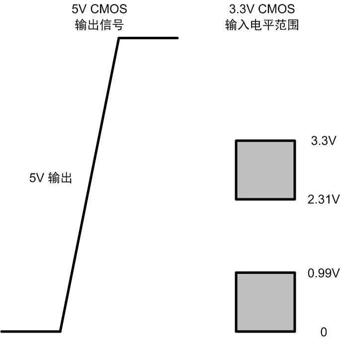
5V device output high level may damage the 3.3V device input interface.
As shown in Figure 2, the output high level signal of the 5V device is much higher than that of the 3.3V device. If the input pin of the 3.3V device does not support 5V level input, current will flow into the 3.3V device during operation, which will seriously damage the device.

Figure 2 5V signal output, 3.3V signal input
Isolated transceiver selection
Take the CTM1051(A)M series product as an example, the CMOS technology chip used in it has the pin level as shown in Figure 3, which conforms to the CMOS level standard. When selecting models, the corresponding models should be selected for different MCUs to avoid problems caused by level mismatch. If the MCU is powered by 5V, CTM1051M should be selected; if the MCU is powered by 3.3V, CTM1051AM should be selected.

Figure 3 CTM1051(A)M pin level
actual case
The customer uses an isolated CAN transceiver module of our company, which has been shipped in large quantities, but there are some abnormal phenomena in the application. Abnormal products are manifested as intermittent communication failures on the CAN bus. When the product is in a high temperature environment (such as 65°C), it can be repeatedly powered on to reproduce the communication failure phenomenon.
1. Recurrence exception
Put the abnormal product in the oven at 65℃, and test the following signals: MCU power supply, TXD, CAN differential, CAN module power supply. When no abnormality occurs, the waveforms of each point are shown in Figure 4. It can be seen that the MCU is powered by 3.3V, the voltage is stable at about 3.2V, the power supply of the CAN module is stable at about 5.07V, and the CAN differential waveform corresponds to the TXD signal without exception.
Repeatedly power on the abnormal board, a large number of error frames appear on the CAN bus, and the problem recurs. When abnormal, the waveform of each point is shown in Figure 5. The MCU power supply voltage and the CAN module power supply voltage fluctuate at the same time, and abnormal bits appear. When the abnormal bit occurs, the power supply of the MCU drops to 3.08V, and the power supply of the CAN module rises to 5.19V.
Carefully observe the abnormal bit waveform, as shown in Figure 6, it is found that when TXD becomes high, the CAN differential level does not follow the change, and when a small noise spike appears on TXD again, the CAN differential level becomes a recessive level. . Combined with the situation that the power supply voltage of the MCU drops and the power supply of the CAN module rises instead, it is initially determined that the problem is caused by the fluctuation of the power supply voltage, which causes the high level of TXD to be unrecognized.
2. Problem location
Because it is suspected that the TXD level cannot be recognized, test the TXD high level threshold voltage value of the CAN module. Under different input voltages, the test data are shown in Table 3.

Table 3 Abnormal product TXD high level threshold voltage
It can be seen from the test data that under different ambient temperatures, the TXD high-level threshold voltage does not change much. When powered by 4.75V, the threshold is about 2.91V; when powered by 5V, the threshold is about 3.06V; when powered by 5.25V, the threshold is about 3.2V.
As shown in Figure 5, when the abnormal bit occurs, the power supply of the CAN module is 5.19V. At this time, the TXD high level threshold should be about 3.17V, while the power supply of the MCU is only 3.08V, and the IO output voltage cannot reach 3.17V, so it cannot be Identify high level. When the TXD has a noise spike, make the TXD higher than 3.17V for a short time, trigger the internal switching of the CAN module, and the bus differential signal changes.
The above guess is verified here, and it is determined that the cause of the failure is: when the power is turned on at high temperature, the power supply voltage of the MCU and CAN module fluctuates, and the TXD pin of the CAN module cannot recognize the high-level signal generated by the MCU, resulting in the continuous occurrence of error frames. , resulting in interruption of CAN communication.

3. Solutions
After replacing the isolation module with level matching (replacement from 5V isolation module to 3.3V isolation module), the TXD high-level threshold voltage and CAN bus communication level amplitude are shown in Figure 7 below, and they have returned to their normal amplitudes. Communication is normal.

Figure 7 TXD high level threshold and CAN bus level after module replacement