【Introduction】Metal oxide semiconductor field effect transistor (MOSFET) is a field effect transistor (FET) Electronic device. It can act as a voltage controlled current source and is mainly used as a switch or for amplifying electrical signals. The control of the MOSFET is carried out by applying a specific voltage to the gate. When a MOSFET is turned on, current flows from the drain to the source of the MOSFET through a channel formed in the body region (called the bulk or body). Most of the time, the body of a MOSFET is connected to the source, which is why MOSFETs are often referred to as 3-pin devices.
How MOSFETs work
A metal oxide semiconductor field effect transistor (MOSFET) is a field effect transistor (FET) Electronic device. It can act as a voltage controlled current source and is mainly used as a switch or for amplifying electrical signals. The control of the MOSFET is carried out by applying a specific voltage to the gate. When a MOSFET is turned on, current flows from the drain to the source of the MOSFET through a channel formed in the body region (called the bulk or body). Most of the time, the body of a MOSFET is connected to the source, which is why MOSFETs are often referred to as 3-pin devices.
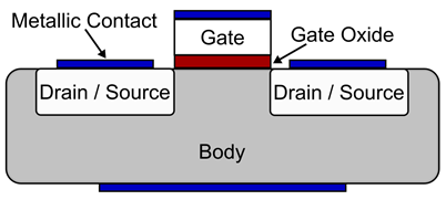
Figure 1: MOSFET
P-channel MOSFET and N-channel MOSFET
A MOSFET is a semiconductor device that is mainly fabricated from P-type or N-type silicon. The difference between these two types of silicon is the charge stored in the doped ions. Dopant ions are charged particles that are implanted into silicon to create charge instabilities that allow the device to be used for electrical purposes. If the silicon region is doped with ions with pentavalent electrons (group V in the periodic table), then an extra electron is released into the semiconductor, so the charge is overall negative (N-type). They donate an electron, so these impurities in silicon are called donor impurities. On the other hand, an element with three electrons in the valence band will lack one electron, which is equivalent to contributing a hole, meaning the total charge is positive (P-type). These impurities are called acceptor impurities. Figure 2 shows the differences between P-type and N-type semiconductor dopants, and their effect on the silicon structure.
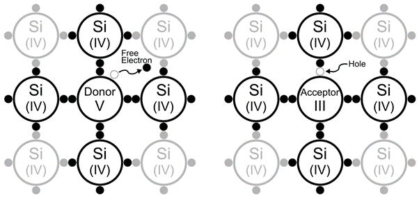
Figure 2: Dopant – Donor or Acceptor Impurity
The simplest MOSFET structure consists of a substrate (which can be either P-type or N-type) and two silicon regions of opposite polarity to the body region, which form the drain and source electrodes (see Figure 3). A MOSFET can be constructed with a P-type substrate and N-type drain and source regions, which means that for current to flow from the drain to the source, the channel must also be N-type. This structure is called an N-channel MOSFET, or NMOS transistor. Conversely, if the substrate is N-type, the channel is P-type, which is called a P-channel MOSFET, or PMOS transistor.
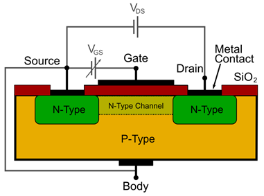
Figure 3: MOSFET structure
Enhancement Mode MOSFET and Depletion Mode MOSFET
MOSFETs get their name from the structure that controls them. Its gate pin is connected to a conductive electrode, which is separated from the substrate by a layer of silicon dioxide or another insulating material. Therefore, when a voltage is applied to the gate, the metal gate generates an electric field, which is transmitted through the oxide layer to the silicon substrate (metal-oxide-semiconductor). The electric field affects the free charge carriers (such as holes or electrons) in the substrate semiconductor and pulls them closer to the gate to form the channel, or pushes them away to destroy the channel.
When an electric field is applied to a semiconductor, it acts on the device’s free charge carriers. Free electrons, uniformly distributed throughout the semiconductor, are attracted to the entry point of the electric field (the gate for a MOSFET with a positive gate voltage). The holes will be dragged in the opposite direction of the electric field to the electrons (see Figure 4), this is called carrier drift, and it logically changes the charge concentration distribution within the semiconductor.
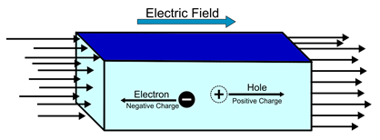
Figure 4: Carrier Drift in semiconductors
The main purpose of a MOSFET is to control the formation of the channel between the drain and source, which either forms or destroys the channel by concentrating the correct charge carriers in the region closest to the gate. Therefore, MOSFETs can be divided into two basic groups: depletion-mode MOSFETs and enhancement-mode MOSFETs.
Depletion-mode MOSFETs have a pre-generated channel (see Figure 5). When a voltage is applied to the gate, the electric field pushes out and depletes the carriers in the channel. Therefore, a depletion-mode MOSFET can be equivalent to a normally-closed switch.
In contrast, the channel in an enhancement-mode MOSFET is only formed when a gate voltage is applied, and it attracts charge and enhances the channel region. Such MOSFETs can be considered normally open switches and are most commonly found in electronic applications. Because if there is a power outage, the switch is closed and current will stop flowing in the Circuit, thus avoiding uncontrolled operation and improving circuit safety. The rest of this article will only refer to enhancement mode N-channel MOSFETs.
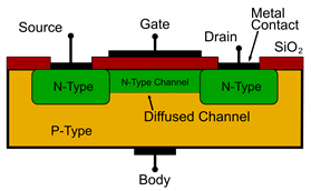
Figure 5: Depletion Mode MOSFET
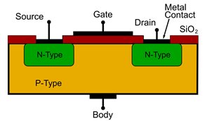
Figure 6: Enhancement Mode MOSFET
MOSFET working area
Based on the above explanation, it is obvious that one of the most important factors in the operation of a MOSFET is the voltage applied to the gate. In fact, the operation of a MOSFET is defined by the voltage (VGS) between the gate and source of the MOSFET. Figure 7 shows how VGS affects the current flowing through the MOSFET. In an enhancement mode N-channel MOSFET, when no voltage is applied between the gate and source, the channel does not exist. This region of operation is called the cut-off region; when the transistor is in this region of operation, no current flows from the drain to the source, which means that the MOSFET behaves like an open switch.
As the gate voltage increases, a channel begins to form, but conduction between the drain and source does not occur until a certain voltage level (called the threshold voltage) is reached. Once the threshold voltage is reached, current begins to flow through the MOSFET. This region is called the saturation region, where the MOSFET acts as a voltage-controlled current source. As the gate voltage increases, so does the current flowing through the switch. The saturation region is mainly used for signal amplification, as small voltage changes in the gate lead to large changes in output current (see Figure 7). The final output current can be used to change the voltage across the resistor, which is the basic working principle of the common source amplifier.
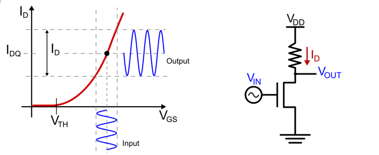
Figure 7: Leakage Current and Gate Voltage
As the gate voltage continues to increase, so does the channel. In the saturation region, the channel is not yet fully connected to the drain-source region, so the voltage between drain and source does not have much effect on operation. However, once the channel is strengthened enough to connect the drain and source (the voltage at this point is called the pinch-off voltage, which is the upper limit of the saturation region), the MOSFET channel is fully enhanced and the transistor behaves as a fully closed switch.
From this point on, the MOSFET can be viewed as a resistor (RDS(ON)) due to the voltage loss between drain and source. This new region of operation is called the ohmic region or linear region, in this region the current across the MOSFET increases and is linearly proportional to the voltage applied between the drain and source of the MOSFET, of course it is still subject to the gate-source voltage limit (see Figure 8).
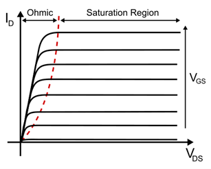
Figure 8: Drain Current and Drain-Source Voltage
Figure 8 provides insight into the usefulness of different workspaces for different applications. As mentioned earlier, the saturation region is best for amplifying the signal, because a small change in gate voltage can result in a large change in current for the same VDS condition. However, since the power dissipation of the MOSFET is defined by the product of the current and the voltage across the MOSFET (VDS), the saturation region is also the worst in terms of power efficiency because it has significant current and drain-to-source voltages.
When the MOSFET is used in switching applications, it must be ensured that the MOSFET operates only as a fully open switch or fully closed switch to reduce power dissipation. In other words, it must work only in the cutoff or linear region and avoid entering the saturation region as much as possible.
Parasitic components in Power MOSFETs
It is important for any electronic device to understand the parasitic elements it contains, which are components that are unintentionally created in the device structure. One of these, the on-resistance, has actually been covered above, but there are other parasitic components in the MOSFET structure (see Figure 9 and Figure 10).
Other passive components present in MOSFETs mainly include various capacitances created by the transistor structure. There are many parasitic capacitances, but the main ones to consider are the capacitances formed between the gate and the drain, and between the gate and the source. These capacitors limit the maximum switching frequency that the device can achieve.
In addition to these passive components, the N+-PN- junction formed by the source, body and drift regions forms a bipolar junction transistor (BJT). This transistor is critical to the safe operation of the MOSFET. If it turns on accidentally, it will cause the MOSFET to go into a “latch-up” state, greatly reducing the maximum blocking voltage. If this voltage is exceeded, the BJT can cause the device to avalanche breakdown, potentially damaging the device without limiting the current. Therefore, the base (body) voltage must be kept as close as possible to the emitter (source) voltage so that the BJT is always off. This is also the reason why the source and base are almost always shorted in power MOSFETs. Also, the source and body are shorted to form a diode called the body diode. It’s not as problematic as BJT, and it’s even useful in some applications.
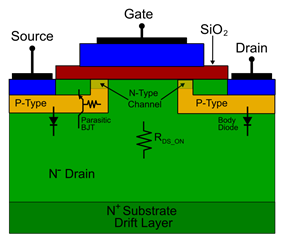
Figure 9: Parasitic Components in Power MOSFETs
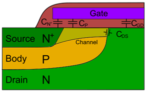
Figure 10: Parasitic capacitance
Power MOSFETs
One of the purposes of using a MOSFET in the design of a power supply application is to ensure that the power supply can operate at high voltages, which also means that it can block high voltages when needed without being broken down. This is achieved by the diode effect formed between the N-Si of the drain and the P-Si of the body. Under bias, the drain-body PN junction acts like a reverse biased diode, forming a space charge region (SCR) and blocking voltage. The higher the bias voltage, the larger the space charge region required for blocking voltage. If the voltage is high enough, the SCR will likely penetrate the space between the drain and source, causing the MOSFET to turn on, which is called reverse breakdown. So the key to working at high voltages seems to be having a very long MOSFET channel. However, making longer transistors is not a viable option for the following reasons:
• Efficiency: A longer channel means higher RDS(ON), which results in higher conduction losses.
• Size: Longer channels will take up more space and will reduce the integration capability of the MOSFET.
For these reasons, power MOSFETs are not built with the traditional MOSFET structure we are used to seeing (see Figure 5), but are built with a vertical structure with the source and gate on the top plate and the drain on the bottom (see Figure 11). .
Since the depth of the transistor poses no manufacturing issues, the depletion region can be as long as needed, which only increases conduction losses. By connecting the MOSFET drains to the entire metal backplane, it is easier to parallel these MOSFETs to increase current capability.
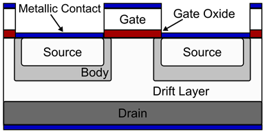
Figure 11: Vertical MOSFET structure
As mentioned earlier, the main energy loss of a MOSFET transistor comes from switching or conduction. Switching losses can be minimized by using fast switching transistors and employing soft switching, but reducing conduction losses is almost entirely dependent on the MOSFET structure, especially the on-resistance, or RDS(ON).
The value of the on-resistance depends on the length of the channel and the carrier concentration of the semiconductor. Of course, the higher the voltage, the stronger the electric field and the larger the depletion region (see Figure 12). Since the depletion region cannot penetrate the entire channel, the depth must be increased. However, increasing the length of the semiconductor has a significant negative impact on the on-resistance, hence the emergence of punch-through semiconductors.
In this type of semiconductor device, the N region in the drain is divided into two parts of different doping density: an N+ region with a very high doping density, and a low density region called the drift layer. Due to the doping gradient between the two regions, the electric field created by the reverse bias is no longer triangular. Instead, it can “punch through” the confinement of the drift region, forming a rectangle (see Figure 13). In this way, the device will allow a higher maximum blocking voltage without having to increase the channel length.
However, the low doping concentration of the drift layer has a negative effect on the semiconductor conductivity of this region, which limits the effect on the on-resistance.
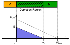
Figure 12: Non punch-through semiconductor
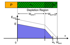
Figure 13: Punch-through semiconductor
MOSFET Safe Operating Area (SOA)
Like all devices, MOSFETs have limitations on their operating conditions. These limitations are primarily related to the maximum voltage and current combination they can operate at before breakdown. To better reflect these constraints, most MOSFET data sheets provide a safe operating area (SOA) diagram (see Figure 14).
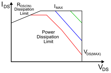
Figure 14: MOSFET Safe Operating Area (SOA)
The upper limit of the safe operating area is determined by the maximum current that can flow through the device. The maximum current is limited by the RDS(ON) of the device because the current flowing through the MOSFET channel (and thus the resistance) generates heat that can cause damage to the device.
The vertical right-hand limit of the SOA is determined by the maximum voltage that the MOSFET can block without breaking down and causing conduction. This depends on the MOSFET’s structure, channel length, and materials used in fabrication, as described in the previous section.
The diagonal limit in the upper right corner of the SOA represents the ability of the MOSFET to maintain operation in the saturation region. The combination of current and voltage in the switch occurs primarily at saturation, where the MOSFET dissipates power, which must then be dissipated as heat. If the product of current and voltage across the MOSFET is too high, excess heat can damage the device.
The lines in the upper right corner of the SOA indicate power consumption limits. These lines show that the dissipation limit of the MOSFET varies with the percentage of time the transistor finds itself in saturation.
If the MOSFET is at a DC voltage, there will be constant current and voltage across the MOSFET and the device will continue to heat up, which greatly limits its ability to dissipate the energy produced. However, if the MOSFET is turned on and off, the device only heats up for a short period of time, so it can withstand higher currents and voltages. The shorter the time to stay on, the higher the voltage and current can be, at this point only limited by the maximum current and voltage.
in conclusion
MOSFETs are an integral part of almost all electronic systems. This drives continuous innovation in MOSFET structures, new materials continue to emerge, circuit designs continue to overcome current physical limitations, and transistors become smaller and smaller. MPS has made an extremely important breakthrough in this field, and its power conversion Modules have power switches that can withstand continuous output currents up to 100A, such as the MPM3695-100. To learn more, visit the MPS website and see related technical articles, reference designs, and application notes.
The Links: PM300DSA060 BSM100GAR120DN2