IGBT (Insulated Gate Bipolar Transistor) is a composite fully-controlled voltage-driven power semiconductor device composed of BJT (Bipolar Transistor) and MOS (Insulated Gate Field Effect Transistor), which combines the high input impedance of MOSFET and GTR The low conduction pressure drop has two advantages. IGBT combines the advantages of the above two devices, with high voltage resistance, low driving power, reduced saturation voltage, fast switching speed, and low switching loss. It is very suitable for use in converter systems with DC voltages of 600 V and above, such as AC motors and switches. Power supply, lighting Circuit, traction drive. At present, IGBT is one of the core technologies in the field of green economy. The specifications are used in aerospace, new energy, rail transit, industrial frequency conversion, smart grid and other fields. As the key core component of automatic control and power conversion, IGBT is an indispensable power “core”. The use of IGBTs for power conversion can improve power efficiency, improve power quality, and achieve an energy-saving effect of 30% to 40%. Even if the traditional equipment is modified with IGBT technology, the average power saving rate can still be increased by 20%.In addition, IGBT is also a key element to realize energy conversion. New energy sources such as photovoltaic power generation, wind power generation, and solar power generation must use IGBT products to transmit electrical energy to the grid.[1-4].
1 Analysis and study of effective mechanism
1.1 Analysis of non-destructive testing of failed devices
1.1.1 X-ray transmission analysis
There is no damage on the surface of the failed IGBT. The multimeter tests that pins 1, 2, and 3 are short-circuited. There is no abnormality in the X-ray transmission of the internal IGBT chip gold wire welding. There are burnt points on the surface of the chip (Figure 1).

Figure 1 IGBT X-ray transmission picture
1.1.2 Unpacking analysis
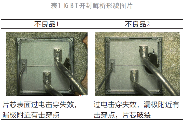
The main board failed IGBT was unpacked and analyzed. The internal chip surface has burn marks. The IGBT failures are all active area (active area) damaged by high energy. The analysis is mainly due to over-electric breakdown failure, as shown in Table 1.

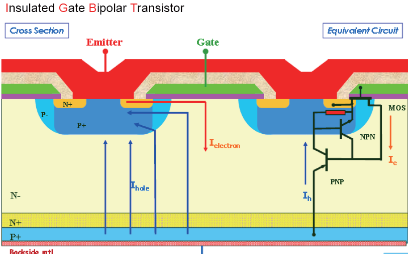
1.1.3 IGBT structure description
The equivalent circuit of insulated gate bipolar transistor IGBT is shown in Figure 2.

Figure 2 IGBT structure description
1.1.4 Failed IGBT application circuit
As shown in Figure 3, the red frame is the rectifier and filter part of the PFC circuit. The C401 capacitor has the function of filtering and suppressing EMI. The PFC main circuit part is composed of PFC inductor L3, IGBT and fast recovery diode D901. When the IGBT is turned on, the inductor L3 is charged, and when the IGBT is turned off, the inductor L3 releases energy. The structure diagram of IGBT application circuit is shown in Figure 3.
2 Failure cause and failure mechanism analysis
After testing the ESD capability of failed IGBT devices, testing and analysis of extreme parameters (ultimate withstand voltage, SOA safe operating area, switching loss,), application environment, drive circuit design, whole machine working waveform analysis, and thermal design analysis, it is found that there are many shortcomings. The summary is summarized as follows. 1) The IGBT gate ESD level is low. After testing the IGBT gate ESD level, the ST IGBT gate ESD level is 3 400 V on average, and the minimum is only 2 900 V. Electrostatic discharge damages the IGBT easily during the production process. Table 2 shows the comparison results of the electrostatic capability test of ST IGBT with Renesas and Farikod (Editor’s Note: Acquired by ON Semiconductor in 2016).
2) Over-voltage event (RBSOA safe working area) of IGBT exceeding the absolute maximum value and latch-up effect cause IGBT failure. After analysis, it is related to the manufacturer’s test. The manufacturer’s test standards are relatively loose, and there is no effective screening for some materials that are discrete at the edge. Excluding, in the overload environment, in the environment of poor power quality, the IGBT latch-up effect is likely to cause breakdown and explosion failure. The manufacturer did not implement the chip latch-up effect test screening in the chip core test link.
3) The IGBT application circuit design has defects. Under special conditions, there is a negative voltage detected. In the PFC circuit, if there is a negative voltage across the IGBT and there is no diode freewheeling, it will damage the IGBT and cause breakdown failure.
4) IGBT gate withstand voltage test found that there are differences between IGBT and two manufacturers’ drive chips. Toshiba IGBT gate withstand voltage is 25~27 V, ST IGBT gate withstand voltage is 24 V, and TC4427 drive chip has a limit withstand voltage 23 V, IR4427 driver chip ultimate withstand voltage 25~27 V. The withstand voltage of TC4427 IGBT driver chip is low, which is lower than the actual working voltage of 24 V Zener diode. When the gate voltage has abrupt fluctuations, the overvoltage shock will break down the TC4427 chip, causing the 24 V Zener diode to actually have no operating voltage. .The selection of the Zener diode is unreasonable, and the withstand voltage level of the Zener diode needs to be reduced. The ultimate withstand voltage level of TC4427 IGBT driver chip is 22 V, and the test data is shown in Table 3.

The voltage regulator tube of the IGBT drive circuit is selected as 24 V, and a large transient voltage appears on the pin Vout of TC4427. When the air conditioner unit is turned off, the actual detection of the IGBT drive waveform shows that the maximum pulse voltage is about 24 V, which is better than the TC4427 specification. The maximum value of 22 V in the book is 2 V higher. If the pulse voltage exceeds the maximum value, the reliability or service life of the device may be affected. The voltage regulator tube value of 24 V is selected based on the protection IR4427, which cannot effectively protect the TC4427. Need to change the regulator tube value to 22 V, increase the power of the regulator tube, so as to effectively protect the TC4427 from overvoltage impact damage. The IGBT gate limit withstand voltage test is shown in Figure 5~ Figure 6. It can be seen that ① GE breakdown voltage: ST is obviously lower than Toshiba. ② EG breakdown voltage: ST is obviously lower than Toshiba.
TC4427 chip limit voltage test, TC4427 chip VCC test shows the breakdown inflection point at 18~19 V for the first time. With the increase of applied voltage, the breakdown voltage increases. The overall test chip breakdown voltage roughly ranges between 21~23 V.
5) The heat dissipation efficiency of the module is poor. The heat sink uses metal wire drawing, which has a large surface roughness (0.15 mm), which affects the heat dissipation efficiency of the module. The wire drawing process appearance of the heat sink is shown in Figure 7, and the roughness needs to be reduced. Change the radiator milling process. Some IGBT failures were analyzed as over-current burnout, and further analyzed as poor heat dissipation and failure of the power device, and the corresponding IGBT screw locking was normal. By checking the matching radiator roughness on the faulty parts, it is confirmed that some of the radiators using metal wire drawing process have poor surface roughness, which can easily lead to poor heat dissipation in some areas during IGBT operation, increased temperature accumulation, and overheating.

Figure 7 Brushed metal appearance of radiator
6) The unqualified electrical clearance between the IGBT copper plate and the radiator leads to the burning problem. After analysis, the size of the silicone sheet is unreasonable, and the staff assembly is different. When the silicone sheet is biased, the electrical gap between the IGBT copper plate and the radiator is unqualified and breakdown Burn out the IGBT. There is a certain gap between the IGBT pin and the boss of the radiator, the silicone sheet is not completely covered, and the electric gap between the IGBT pin and the boss of the radiator is too small, and there is also a hidden danger of over-electricity and ignition. The ignition failure of IGBT is shown in Figure 8. The size of the silicone sheet needs to be increased to ensure effective electrical clearance.


Figure 8 Picture of failed IGBT ignition
3 IGBT working reliability improvement plan
1) Improve the ESD level of the IGBT gate from 3 400 V to 8 000 V. Basically put an end to ESD damage to the IGBT during the production process and cause failure. The test data of ST’s new product ESD level test is shown in Table 4, and the comparison data of IGBT gate ESD test of two manufacturers of AB is shown in Fig. 9.


Figure 9 IGBT gate ESD level test comparison
2) Implement the automotive-grade PPAT screening test standard and add 100% chip latching effect test. The manufacturer implements the chip latching effect test screening during the chip test (adding PPAT test to screen VTH, BVCES, VCESAT parameters). The PPAT test can eliminate any possible outliers or lock-in weaknesses, as shown in Figure 10, and eliminate all discrete materials with quality and reliability problems.
3) A 5 A/600 V freewheeling diode is added inside the IGBT to prevent the possible negative voltage of the IGBT, solve the problem of IGBT failure caused by the reverse negative pressure of the IGBT, and improve the reliability of the IGBT working in a complex environment.
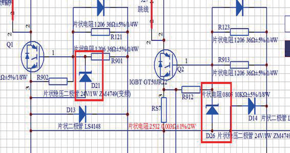
4) Re-selection of IGBT gate drive zener diode, and change the working voltage from 24 V to 20 V.
Adjust the voltage stabilization value of the zener diode in the front stage to ensure the redundancy of the work. The TC4427 chip’s limit working voltage is greater than 22 V, and the actual test average working limit withstand voltage value is 23 V. The IGBT drive circuit uses a voltage stabilizer diode of 24 V, which cannot effectively drive the IGBT protection circuit, and the drive chip fails, resulting in IGBT breakdown. Test the limit working voltage of each batch of TC4427 chip (IGBT driver chip) is greater than 22 V (in accordance with the specification), generally less than 24 V. Analysis of the 24 V Zener diode in the circuit design can be better protected after changing to 20 V The driver chip and IGBT in the circuit are shown in Figure 11.

Figure 13 IGBT drive circuit diagram
5) The driver chip is changed to the IR4427 chip, the gate withstand voltage of this chip is relatively high, the withstand voltage of TC4427 is 22~23 V, and the ultimate withstand voltage of IR4427 is 25~27 V.
6) Improve the heat dissipation efficiency, change the heat sink processing technology, change the metal wire drawing process to the milling process, improve the roughness of the heat sink assembly surface, reduce from 0.15 mm to 0.05 mm, and greatly improve the IGBT heat dissipation efficiency. The overall temperature rise of the IGBT is reduced by 5 ℃.
7) The size of the silicone sheet is lengthened, and the size of the silicone sheet is changed to prevent the IGBT and the radiator from being burnt due to contact with the radiator due to the too small size of the silicone sheet. It is 8 mm longer than before, which can better wrap the bottom of the IGBT body and the IGBT pins to prevent leakage of the silicone sheet and the heat sink, and abnormal ignition caused by insufficient electrical clearance.
8) Choose a low thermal resistance silicone sheet to improve the heat dissipation efficiency of the IGBT. After testing the temperature rise and heat dissipation efficiency of the new material IGBT, the temperature rise can be reduced by about 5 ℃. Reduce the failure probability of IGBT thermal breakdown and improve the reliability of IGBT operation.
4 Summary and significance of rectification
This article combines a large number of failure product analysis and circuit design analysis, and the results of the IGBT failure cause and failure mechanism analysis show that: after the IGBT failure analysis and the IGBT working circuit failure analysis, the whole machine related waveform detection, thermal design analysis, and IGBT limit parameter detection comparison It is found that IGBT failure is caused by many reasons. IGBT has shortcomings in device selection, device reliability, latch-up effect, drive control, ESD capability, etc. After analyzing and demonstrating one by one, improve the reliability of IGBT from the aspects of IGBT itself and circuit design. .
references:
[1] Wang Rui. Research on high-power IGBT gate drive circuit[J].Electrical Automation, 2014(3):115-117.
[2] Yang Hongsheng, Song Guomeng, Wang Xiong. Research on the Influence of Air Gap in the Contact Interface Between IGBT Module and Heat Sink on Heat Dissipation[J]. Locomotive Electric Drive, 2020(1): 18-21, 33.
[3] Yin Xin. Research on IGBT turn-off overvoltage based on gate control[J].Power Technology, 2016(3):680-683.
[4] Tang Yong. IGBT reliability and online evaluation at high temperature[J].Electrical Engineering Figure 13 IGBT drive circuit diagram report, 2014(6):17-23.