MOSFET, which stands for Metal Oxide Semiconductor Field Effect Transistor, is composed of the abbreviations MOS (Metal Oxide Semiconductor) and FET (Field Effect Transistor). It operates by applying a voltage to the metal gate (M – aluminum) and generating an electric field effect across the oxide layer (O – silicon dioxide) to control the conduction channel of the semiconductor (S). Due to the insulation provided by the SiO2 layer between the gate and source/drain, MOSFET is also referred to as an Insulated Gate Field Effect Transistor (IGFET). The term “power MOSFET” often refers to the Insulated Gate MOSFET (Metal Oxide Semiconductor FET), commonly known as Power MOSFET. In reality, field-effect transistors can be categorized into two types: junction-type and insulated-gate type.
Power MOSFETs are mainly used as switches and drivers, operating in a switching state. They can handle voltage ratings from a few tens of volts to over a thousand volts and handle currents ranging from a few amperes to several tens of amperes. Most power MOSFETs are of the enhancement type, characterized by excellent switching characteristics.
Classification of MOSFETs:
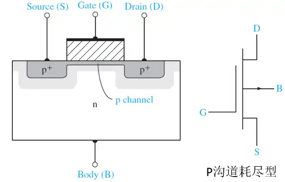
MOSFETs can be classified based on the type of conduction channel: P-channel and N-channel. They can also be categorized according to the gate voltage magnitude: depletion mode – where a conductive channel exists between source and drain even at zero gate voltage; enhancement mode – a conductive channel forms only when the gate voltage is greater (or smaller for P-channel devices) than zero. Power MOSFETs are primarily of the N-channel enhancement type.


MOSFET Structure and Principles:
(Using N-channel enhancement mode as an example)
The structure of an N-channel enhancement mode MOSFET is illustrated in Figure 5. It employs a lightly doped P-type silicon substrate as the base, and through diffusion processes, creates two highly doped N+ regions. These regions become the source (S) and drain (D) terminals. A layer of SiO2 insulation is created on the semiconductor, followed by a layer of aluminum (Al) to form the gate (G) electrode. Typically, the substrate is connected to the source terminal. This arrangement creates a capacitor-like structure with the gate and substrate acting as plates and the insulating layer in between. When the gate-to-source voltage changes, it affects the amount of induced charge near the insulating layer, controlling the drain current.

MOSFET Operation Principle:
(Using N-channel enhancement mode as an example)
When no voltage is applied between the gate and source (VGS = 0), a reverse-biased PN junction forms between the source and drain. Regardless of the polarity of VDS, at least one PN junction is reverse-biased, preventing a conductive channel from forming.
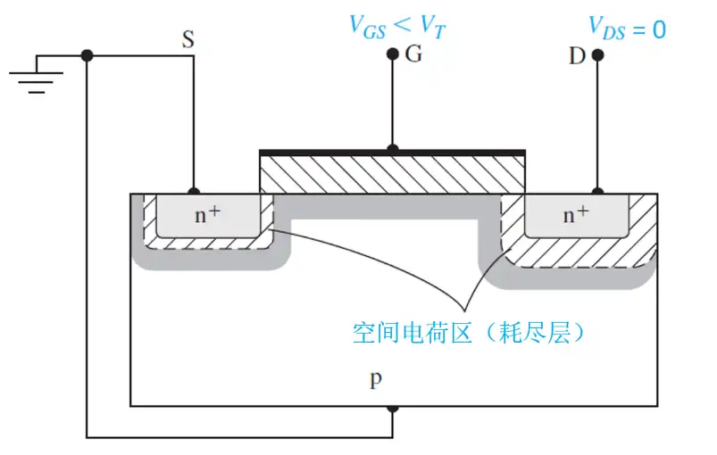
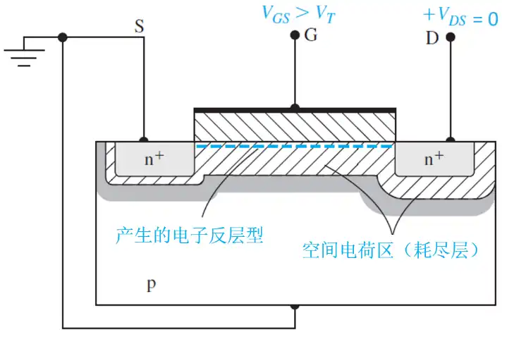
When UDS = 0 and UGS > 0, the presence of SiO2 prevents gate current. However, the gate metal layer accumulates positive charges, repelling holes on the P-type substrate side near SiO2 and creating a depletion layer (as shown in Figure 6).
As UGS increases, the depletion layer widens, and free electrons from the substrate are drawn to the region between the depletion layer and the insulator, forming an N-type region known as the inversion layer (as shown in Figure 7). This inversion layer constitutes the conductive channel between drain and source. The voltage UGS at which this channel just forms is called the threshold voltage (UGS(th))/VT. Higher UGS results in a thicker inversion layer and lower channel resistance.
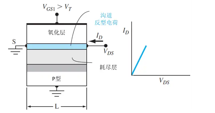
When VGS > VT and VDS is relatively small, the basic MOS structure is depicted in Figure 8-1. The thickness of the inversion channel layer indicates the relative charge density. At this point, the charge density is constant along the channel length. The corresponding ID-VDS characteristic curve is shown in Figure 8-1.
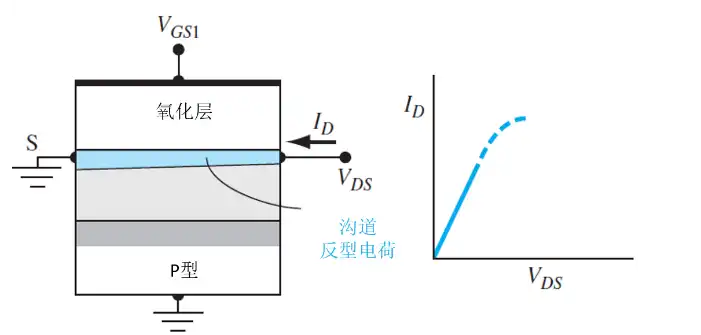
As VGS > VT and VDS increases, the voltage drop across the oxide layer near the drain diminishes due to increased drain voltage. This reduces the charge density of the inversion layer near the drain. Consequently, the channel conductance near the drain decreases, resulting in a reduced slope of the ID-VDS characteristic curve (as shown in Figure 8-2).
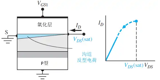
When VGS > VT and VDS increases to the point where the voltage drop across the oxide layer near the drain equals VT, the charge density of the inversion layer near the drain becomes zero. As a result, the drain-end conductance becomes zero, yielding a zero slope in the ID-VDS curve, referred to as pinch-off (as shown in Figure 8-3).
When VGS > VT and VDS > VDS(sat), the point where the inversion charge is zero moves towards the source. Further increases in UDS extend the pinch-off region, and most of the increase in UDS is used to overcome the resistance of the pinch-off region to drain current, resulting in a constant drain current ID. This corresponds to the saturation region in the ID-VDS curve (as shown in Figure 8-4).
MOSFET Characteristics:
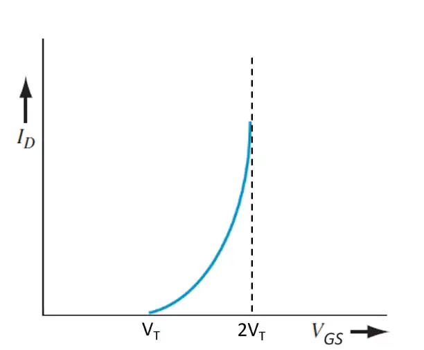
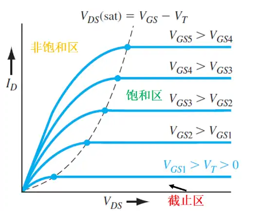
The relationship between drain current ID and gate-source voltage UGS is referred to as the transfer characteristic of a MOSFET. When ID is relatively large, the relationship between ID and UGS is approximately linear, and the slope of the curve is defined as transconductance (Gfs). With increasing VGS, the slope of ID also increases. This is due to the thicker inversion layer forming with higher VGS, resulting in lower channel resistance and faster increase in ID. MOSFETs have three operational regions: the cut-off region, saturation region, and non-saturation region, corresponding to the output characteristic curves as shown in Figure 10. If a power MOSFET operates in a switching state, it transitions between the cut-off and non-saturation regions.
